Light fields made up of tiny LEDs are opening up completely new ways of exploring the micro world – for researchers and the general public alike.
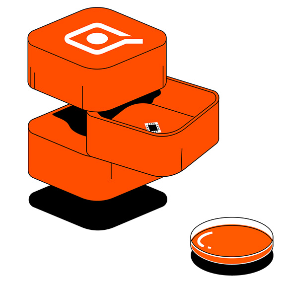
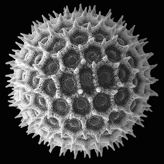
Professor Andreas Waag is the only physicist in the room. He is one of a group of scientists from various disciplines at the Laboratory for Emerging Nanometrology (LENA) in Braunschweig, Germany. They are all gazing intently at a screen showing pollen, magnified 10,000 times and in sharp focus right to the very edges. On a table, there is an eleven-centimeter tall bright red cube in the middle of which is a Petri dish containing pollen from the neighboring forest. Above the dish is a µLED array, a tiny structured LED; in the bottom section is a sensor. The setup gives some idea of the capabilities of controllable light fields based on µLEDs. It’s the prototype of a robust, low-cost microscope with resolutions that go beyond optical thresholds.
Anywhere, any time
Microscopes have given us a wealth of additional knowledge about us and our environment. What if this technology were to be available anywhere and at any time? It would be possible in the early stages of an illness to determine whether the cause was a virus or bacteria. Infectious diseases would also be easier to track down if a microscope could observe cell growth directly in an incubator. Air purity could always be measured directly on-site – and not in a measuring station a great distance away.
µ-knowledge for all
The team led by Professor Waag is focusing on societal challenges and thinking in terms of concrete applications. The professor himself speaks with enthusiasm: “We know far too little about our immediate environment. Microsensor technology is still too expensive and not widely available. It is mainly reserved for laboratories and universities. We are working here on solutions that will allow the general public to gain accurate insights into themselves and the environment.” One of the reasons why this can be achieved at LENA is no doubt its interdisciplinary approach to the challenges. Expertise from years of joint semiconductor research with external partners coupled with the experience of various departments in the university flows into product development.
The microscope, for example, is a combination of photonics, electronics, mechanical engineering, and software development, with a requirement profile defined by biologists and environmental scientists. This prototype of a revolutionary microscope, destined to provide a broad public with easy access to knowledge about ourselves and our environment, is essentially based on two principles: overcoming the optical resolution limit and miniaturizing the fundamental technology.
Overcoming the diffraction limit
A conventional microscope, which works with visible light, has a resolution limit of approximately 200 nanometers. That roughly corresponds to one-250th of the thickness of a human hair. The principle of decoupling the resolution from the wavelength of light and exploring the nano world beyond optical limits was achieved with the stimulation emission depletion microscope (STED), which was awarded the Nobel Prize in 2014. Since then, although there are basically no limits to delving into the micro world, the challenges are immense. All attempts to improve on the principle did not solve the main problems: namely large space requirements, temperature dependence, and high production costs.
The technology had to be rethought. But there was no need to reinvent the wheel – all that was required was some lateral thinking. Gallium nitride LED technology, which revolutionized general lighting a few years ago, paved the way here, too. But first, the LEDs had to be miniaturized down to the micrometer level, combined in large numbers in an array, and controlled individually.
Structured, selective illumination of objects allows them to be analyzed in 3D. The new limit for the resolution of objects is then only the spacing between the LEDs and no longer the wavelength of light as a result of the diffraction limit. Time-shifted point-for-point illumination from different angles enables the object to be accurately calculated. The result is a precise, three-dimensional shadow image of the object, such as pollen in this case or particles in the air. A major advantage of this type of microscopy, apart from its small size and robustness, is its resistance to temperature – it would be the first lens-free solution capable of being used directly in a laboratory incubator. Images of living cells could be captured in real time under natural conditions and with many different wavelengths. This would provide significantly more information than with conventional microscopes.
Contactless scanning
The necessary LED chip technology is already available – not least thanks to twelve years of research involving a team of experts at OSRAM Opto Semiconductors in Regensburg. Waag and his team are now working on miniaturizing the µLED arrays, shown here as “Structured Micro-Illumination Light Engines” (SMILE for short) even further. The intention in the medium term is for these to cover the entire bandwidth of wavelengths. Waag, who is also the spokesperson for the Excellence Cluster Quantum Frontiers, provides a forecast of the possibilities: “Controlling light at the micro level is leading to new mobile, energy-efficient, contactless sensors. In an ideal case, such SMILE microLED arrays would cover customizable wavelengths from infrared to ultraviolet. They would then be able to “scan” various properties of our environment and our bodies with high precision, illuminating them in the truest sense.”
QubeDot, a spin-off startup operating in LENA, is working on market-compatible development of the new technology. There, they believe that “the microscope for all” will change health care and environmental sciences in particular. It may well take the form of a pen. Instead of an ink cartridge, there would be a vial that could be filled with body fluids to be analyzed for viruses or bacteria. Or it might look like a pocket-size hinged iPod for measuring the number of particles in the air. Anything with a display could be used as an output screen – a smart watch, a smartphone, or a PC.
So much untapped potential
The possibilities of this chip technology based on quantum physics are fueling dreams. The technology has the potential for reinventing even more than microscopy. Further into the future, SMILEs could be used as new kinds of light sources in biomedical imaging and sensor applications. Specifically, neuroscientists could convert optical signals from the µLED arrays into electrical signals in the cell in order to address entire networks of nerve cells with complex signal forms. And looking even further ahead, the ability of these light fields of incredibly tiny LEDs to control individual ions by optical means could even pave the way for quantum computers.