ams AS5966 CT Sensor Chip

×

Description

Product status: Pre-Production

The AS5966 is a sensor chip for CT detectors that combines the photodiodes and the readout circuit on a single CMOS chip by using through silicon vias (TSV). This sensor solution, which integrates an array of 10 x 8 photodiodes and an 80-channel ADC on top of each other, allowing the assembly of the pixel array on four adjacent edges of the device.

Featuring on-chip photodiodes, the AS5966 offers high performance for CT detectors across all segments. The TSV technology allows for very low parasitic capacitance between back-side illuminated photodiode and the ADC front-end. This leads to superior image performance that can be achieved because of the very low input-related noise of 0.38 fC at a maximum input current range of 335 nA. The ultra-low power consumption of 0.94 mW/pixel reduces self-heating effects and lowers the overall cost of cooling the system.

The digital data readout can be accessed via a 15 MHz CMOS level interface. An appropriate separate interface is used for device configuration as well as data output operation. An integrated temperature sensor enables monitoring of the junction temperature.

Its 4-side buttability allows to place AS5966 on all four adjacent edges of the IC that enables a wide range of CT detector designs from 20 mm to 160 mm of Z-coverage in ISO center. The AS5966 is directly assembled on a substrate using a soldering and underfill process for manufacturing of the CT tile. AS5966 has a pixel dimension of 1.1x1.02 mm², pixel dimensions can be customized on request.

Watch the product video

Gain deeper insights about Through Silicon Via (TSV)

Details

Features

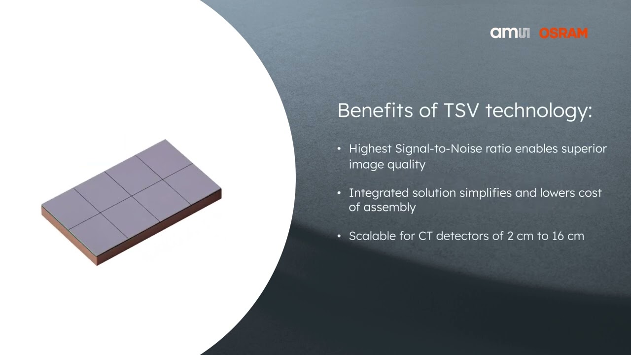
  • Integration of 80-channel ADC and photodiode array in one ASIC using TSV technology
  • Lowest input related noise of 0.38 fC at 335 nA input range
  • Low power dissipation of 0.94 mW/pixel at 195.5 μs
  • Integration time of min. 195.5 μs
  • 15 MHz CMOS level interface for data streaming and device configuration

Benefits

  • 4-Side Buttable ASIC to achieve Z-coverage of 2 cm to 16 cm in ISO center
  • Pixel size 1.1 x 1.02 mm². Customization of pixel dimensions on request
  • No need of X-ray shield for ADC protection

Parameters

Channels
input
80
Integration time
min.
195.5 µs
Input related noise
0.38
Power consumption per channel
min.
0.94 mW
Resolution
20 bit
Package
WLCSP
Function
x-ray sensing

Downloads